Menu

Understanding the Basics of Semiconductor Inspection Optics: A Comprehensive Guide
Release time:
2026-07-05
Understanding the Basics of Semiconductor Inspection Optics Table of Contents 1. Introduction to Semiconductor Inspection Optics 2. Importance of Inspection Optics in Semiconductor Manufacturing 3. Key Components of Inspection Optics 4. Types of Inspection Optical Systems 5. Principles of Optical Inspection 6. Advancements in Semiconductor Inspection Technologies 7. Challenges in Se
Understanding the Basics of Semiconductor Inspection Optics
Table of Contents
- 1. Introduction to Semiconductor Inspection Optics
- 2. Importance of Inspection Optics in Semiconductor Manufacturing
- 3. Key Components of Inspection Optics
- 4. Types of Inspection Optical Systems
- 5. Principles of Optical Inspection
- 6. Advancements in Semiconductor Inspection Technologies
- 7. Challenges in Semiconductor Inspection
- 8. Future Trends in Semiconductor Inspection Optics
- 9. Frequently Asked Questions
- 10. Conclusion
1. Introduction to Semiconductor Inspection Optics
In the realm of semiconductor manufacturing, **inspection optics** play a crucial role in ensuring product quality and performance. As the demand for smaller, more powerful electronic devices continues to rise, so does the need for sophisticated inspection techniques. This section provides an overview of semiconductor inspection optics, highlighting its importance in the manufacturing process.
2. Importance of Inspection Optics in Semiconductor Manufacturing
The semiconductor industry operates in a highly competitive environment where precision and quality are paramount. **Inspection optics** are vital for detecting defects at various stages of semiconductor fabrication, including photolithography, etching, and deposition. By utilizing advanced optical systems, manufacturers can enhance yield rates, reduce waste, and ultimately improve product reliability.
Why Inspection Matters
Defects in semiconductor devices can lead to catastrophic failures, affecting both performance and longevity. Efficient inspection processes help identify these issues early, allowing for timely corrective actions. The integration of optical inspection systems not only streamlines manufacturing processes but also ensures compliance with industry standards.
3. Key Components of Inspection Optics
Understanding the various components of **inspection optics** is essential for grasping how these systems function. The fundamental components include:
- Light Sources: These are essential for illuminating the semiconductor surfaces. Common types include laser diodes and LED arrays.
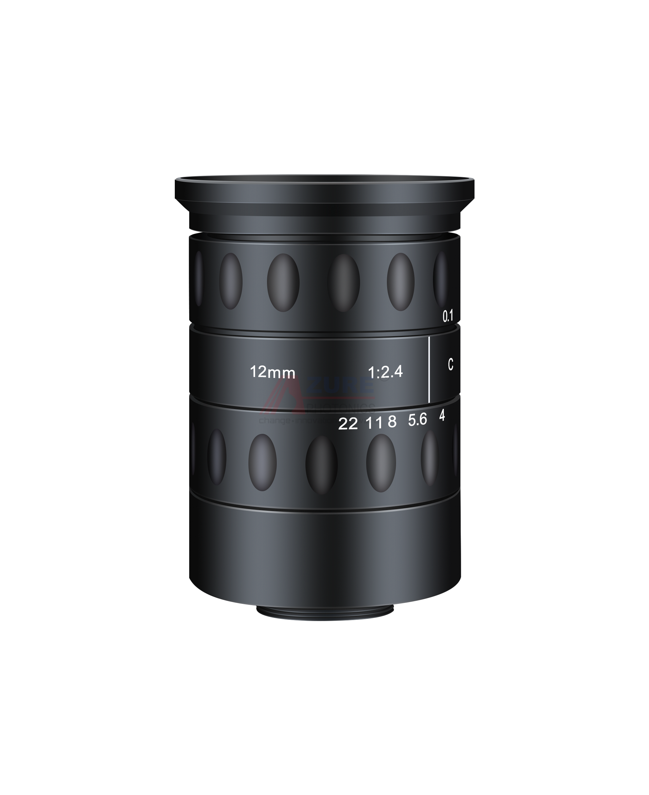
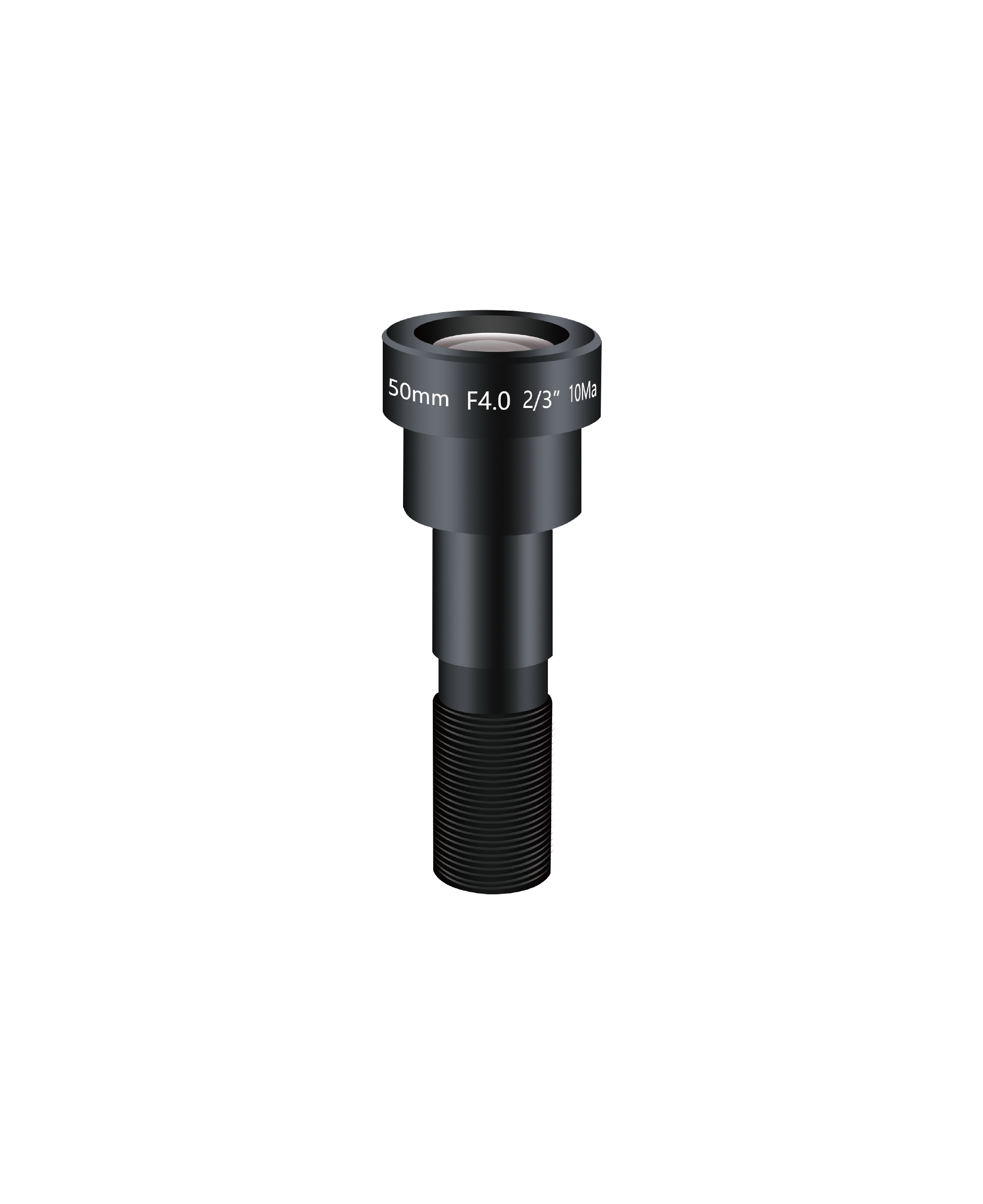
- Optical Lenses: Lenses focus and direct light onto the target, enhancing image clarity and detail.
- Detectors: These convert light signals into electrical signals for processing. CCD and CMOS sensors are commonly used in inspection systems.
- Imaging Systems: These systems capture images of the semiconductor surfaces for analysis and defect detection.
4. Types of Inspection Optical Systems
Several types of **inspection optical systems** are employed in semiconductor manufacturing. Each type serves specific purposes and offers unique benefits.
4.1. Bright Field Inspection
Bright field inspection uses direct illumination to highlight defects against a uniformly lit background. This method is effective for detecting surface defects and is commonly used in initial wafer inspections.
4.2. Dark Field Inspection
In contrast to bright field inspection, dark field inspection uses oblique lighting to enhance the visibility of defects. This technique is particularly useful for identifying particles and contamination on the wafer surface.
4.3. Phase Shift Inspection
Phase shift inspection offers high-resolution imaging by utilizing phase contrast techniques. This method is adept at detecting sub-wavelength defects, making it indispensable in advanced semiconductor fabrication.
4.4. Reflective and Transmissive Systems
Reflective systems utilize mirrors and lenses to gather light reflected from the surface, whereas transmissive systems analyze light passing through the material. Both systems have applications depending on the specific inspection requirements.
5. Principles of Optical Inspection
The principles underlying **optical inspection** are rooted in the behavior of light and its interaction with materials. Key principles include:
5.1. Resolution and Magnification
Resolution refers to the ability to distinguish between two closely spaced objects, while magnification increases the apparent size of an object. Both factors are critical in optical inspection for identifying minute defects.
5.2. Contrast and Signal-to-Noise Ratio
Contrast is the difference in luminance between the object and the background, while the signal-to-noise ratio (SNR) measures the level of desired signal compared to background noise. Higher contrast and SNR improve defect detection accuracy.
6. Advancements in Semiconductor Inspection Technologies
The field of semiconductor inspection optics is rapidly evolving, driven by advancements in technology and increasing complexity of semiconductor devices. Notable advancements include:
6.1. Machine Learning and AI Integration
Integrating machine learning and artificial intelligence into inspection systems enhances defect detection capabilities. These technologies can analyze large datasets, identify patterns, and improve inspection algorithms over time.
6.2. High-Resolution Imaging
Recent innovations in imaging sensors have led to higher resolution capabilities, enabling the detection of defects at nanometer scales. This is essential for maintaining the quality of advanced semiconductor devices.
6.3. Automation and Robotics
Automation in the inspection process minimizes human error and increases efficiency. Robotic systems can handle the inspection tasks, allowing for faster throughput and improved accuracy.
7. Challenges in Semiconductor Inspection
While **inspection optics** have greatly advanced, several challenges remain in their implementation. These include:
7.1. Complexity of Defects
As semiconductor structures become more intricate, the types of defects are also evolving. Identifying and classifying these new defects requires continual adaptation of inspection technologies and methodologies.
7.2. Cost of Advanced Systems
The initial investment in advanced optical inspection systems can be substantial. Balancing cost and performance while maintaining quality is a significant challenge for many manufacturers.
8. Future Trends in Semiconductor Inspection Optics
The future of **semiconductor inspection optics** is bright, with several key trends expected to shape its evolution:
8.1. Increased Use of 3D Imaging
As semiconductor devices become more complex, 3D imaging technologies will become increasingly important for accurate inspection and analysis. This will provide a more comprehensive understanding of defects.
8.2. Sustainability and Eco-Friendly Practices
With growing environmental concerns, the industry is leaning toward sustainable practices. This includes developing eco-friendly materials and processes for optical inspection systems.
8.3. Enhanced Collaboration between Manufacturers and Researchers
Collaboration between semiconductor manufacturers and research institutions will foster innovation in inspection technologies, leading to more effective solutions for defect detection.
9. Frequently Asked Questions
9.1. What is semiconductor inspection optics?
Semiconductor inspection optics refers to the optical systems used to detect defects in semiconductor materials and devices during manufacturing processes.
9.2. How does optical inspection work?
Optical inspection works by using various light sources and imaging systems to illuminate, capture, and analyze images of semiconductor surfaces for defects.
9.3. What are the main types of optical inspection systems?
The main types include bright field, dark field, phase shift, and reflective/transmissive systems, each suited for specific inspection tasks.
9.4. What challenges do manufacturers face with optical inspection?
Manufacturers face challenges such as the complexity of defects, high costs of advanced systems, and the need for continual adaptation to evolving technologies.
9.5. What is the future of semiconductor inspection optics?
The future includes advancements in 3D imaging, sustainable practices, and increased collaboration for innovation in inspection technologies.
10. Conclusion
In conclusion, understanding the basics of **semiconductor inspection optics** is crucial for anyone involved in the semiconductor manufacturing industry. As technology continues to advance, so will the methods employed for effective inspection. With the integration of machine learning, automation, and sustainable practices, the field is poised for significant growth and evolution. By staying informed about the latest trends and technologies, manufacturers can ensure they remain competitive in this ever-changing landscape.

Building No.15, Haixi Hi-Tech Park, Wulongjiang Avenue,
Shangjie Town, Minhou County, Fuzhou, Fujian 350108, P. R. China.

Scan the code
Online Message
Please describe your needs in detail. We will contact you as soon as possible after receiving your message.
Powered by www.300.cn SEO Privacy Notice